本文使用金属有机物化学气相沉积(MOCVD)法在不同切割角的c面蓝宝石衬底上外延氧化镓(β-Ga2O3)单晶薄膜, 揭示了衬底切割角对外延薄膜晶体质量的影响规律。研究表明, 当衬底切割角为6°时, β-Ga2O3外延膜具有较小的X射线摇摆曲线半峰全宽(1.10°)和最小的表面粗糙度(7.7 nm)。在此基础上, 采用光刻、显影、电子束蒸发及剥离工艺制备了金属-半导体-金属结构的日盲紫外光电探测器, 器件的光暗电流比为6.2×10⁶, 248 nm处的峰值响应度为87.12 A/W, 比探测率为3.5×10¹⁵ Jones, 带外抑制比为2.36×10⁴, 响应时间为226.2 μs。
超宽禁带半导体 氧化镓薄膜 金属有机物化学气相沉积 日盲紫外光电探测器 切割角 外延 ultra-wide bandgap semiconductor β-Ga2O3 film metal organic chemical vapor deposition solar-blind ultraviolet photodetector off-cut angle epitaxy

Author Affiliations
Abstract
1 School of Electronic Science and Engineering, Collaborative Innovation Center of Advanced Microstructures, Nanjing University, Nanjing 210023, China
2 School of Electronic and Information Engineering, Nanjing University of Information Science & Technology Binjiang College, Wuxi 214105, China
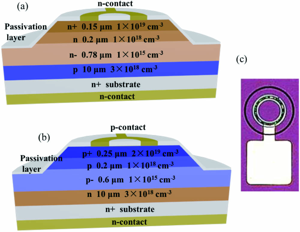
Understanding detailed avalanche mechanisms is critical for design optimization of avalanche photodiodes (APDs). In this work, avalanche characteristics and single photon counting performance of 4H-SiC n-i-p and p-i-n APDs are compared. By studying the evolution of breakdown voltage as a function of incident light wavelength, it is confirmed that at the deep ultraviolet (UV) wavelength region the avalanche events in 4H-SiC n-i-p APDs are mainly induced by hole-initiated ionization, while electron-initiated ionization is the main cause of avalanche breakdown in 4H-SiC p-i-n APDs. Meanwhile, at the same dark count rate, the single photon counting efficiency of n-i-p APDs is considerably higher than that of p-i-n APDs. The higher performance of n-i-p APDs can be explained by the larger impact ionization coefficient of holes in 4H-SiC. In addition, this is the first time, to the best of our knowledge, to report single photon detection performance of vertical 4H-SiC n-i-p-n APDs.
4H-SiC avalanche photodiode electron-initiated ionization hole-initiated ionization Chinese Optics Letters
2021, 19(9): 092501

Author Affiliations
Abstract
Research Institute of Shenzhen and School of Electronics Science and Engineering, Nanjing University, Nanjing 210093, China
The 8 μm thick single-crystalline α-Ga2O3 epilayers have been heteroepitaxially grown on sapphire (0001) substrates via mist chemical vapor deposition technique. High resolution X-ray diffraction measurements show that the full-widths-at-half-maximum (FWHM) of rocking curves for the (0006) and (10-14) planes are 0.024° and 0.24°, and the corresponding densities of screw and edge dislocations are 2.24 × 10⁶ and 1.63 × 109 cm-2, respectively, indicative of high single crystallinity. The out-of-plane and in-plane epitaxial relationships are [0001] α-Ga2O3//[0001] α-Al2O3 and [11-20] α-Ga2O3//[11-20] α-Al2O3, respectively. The lateral domain size is in micron scale and the indirect bandgap is determined as 5.03 eV by transmittance spectra. Raman measurement indicates that the lattice-mismatch induced compressive residual strain cannot be ruled out despite the large thickness of the α-Ga2O3 epilayer. The achieved high quality α-Ga2O3 may provide an alternative material platform for developing high performance power devices and solar-blind photodetectors.
Journal of Semiconductors
2019, 40(1): 012804

Author Affiliations
Abstract
1 School of Electronic Science and Engineering, Nanjing University, Nanjing 210023, China
2 e-mail: wz.xu@nju.edu.cn
3 e-mail: hailu@nju.edu.cn
In this work, a GaN p-i-n diode based on Mg ion implantation for visible-blind UV detection is demonstrated. With an optimized implantation and annealing process, a p-GaN layer and corresponding GaN p-i-n photodiode are achieved via Mg implantation. As revealed in the UV detection characterizations, these diodes exhibit a sharp wavelength cutoff at 365 nm, high UV/visible rejection ratio of 1.2×10⁴, and high photoresponsivity of 0.35 A/W, and are proved to be comparable with commercially available GaN p-n photodiodes. Additionally, a localized states-related gain mechanism is systematically investigated, and a relevant physics model of electric-field-assisted photocarrier hopping is proposed. The demonstrated Mg ion-implantation-based approach is believed to be an applicable and CMOS-process-compatible technology for GaN-based p-i-n photodiodes.
Photonics Research
2019, 7(8): 08000B48

Author Affiliations
Abstract
School of Electronics Science and Engineering, Nanjing University, Nanjing 210093, China
Solar-blind photodetectors are of great interest to a wide range of industrial, civil, environmental, and biological applications. As one of the emerging ultrawide-bandgap semiconductors, gallium oxide (Ga2O3) exhibits unique advantages over other wide-bandgap semiconductors, especially in developing high-performance solar-blind photodetectors. This paper comprehensively reviews the latest progresses of solar-blind photodetectors based on Ga2O3 materials in various forms of bulk single crystal, epitaxial films, nanostructures, and their ternary alloys. The basic working principles of photodetectors and the fundamental properties and synthesis of Ga2O3, as well as device processing developments, have been briefly summarized. A special focus is to address the physical mechanism for commonly observed huge photoconductive gains. Benefitting from the rapid development in material epitaxy and device processes, Ga2O3-based solar-blind detectors represent to date one of the most prospective solutions for UV detection technology towards versatile applications.
Photonics Research
2019, 7(4): 04000381


